


Gas Purifiers Semiconductor
In the ultra-high purity (UHP) environments of semiconductor manufacturing, the margin for error is measured in parts per trillion (PPT). As integrated circuit (IC) nodes continue to shrink toward 3nm and beyond, the sensitivity of fabrication processes to molecular and particulate contamination has reached unprecedented levels. Gas purifiers for semiconductor applications serve as the final, critical gatekeeper in the delivery of process gases, ensuring that bulk and specialty gases meet the stringent cleanliness requirements necessary to maintain high wafer yields.
For engineers and system designers, selecting the right filtration and purification components is not merely a matter of meeting a specification; it is about ensuring the long-term stability of the entire lithography, etching, and deposition ecosystem. This guide examines the technical requirements, engineering considerations, and material standards for gas purifiers in the semiconductor industry.
The Critical Role of Gas Purity in Modern Semiconductor Fabrication
Semiconductor manufacturing relies on a vast array of gases, categorized into bulk gases (such as Nitrogen, Oxygen, Argon, and Hydrogen) and specialty gases (including hydrides, halides, and organometallics). These gases are used in various stages, from creating inert atmospheres to the precise chemical vapor deposition (CVD) of thin films.
Contaminants in these gas streams—whether they are moisture, oxygen, carbon dioxide, or metallic particles—can lead to catastrophic defects. For instance, even trace amounts of moisture in a corrosive gas stream like Hydrogen Chloride (HCl) can lead to rapid corrosion of delivery lines, resulting in particulate generation and system downtime. Gas purifiers for semiconductor processes are designed to remove these contaminants to sub-ppb or even ppt levels, protecting both the process and the hardware.
The integration of high-performance filtration components within these purifiers is essential. While the purifier's chemical media handles molecular contaminants, the mechanical filtration elements must ensure that no media migration occurs and that any incoming particulates are captured with near-perfect efficiency.
Technical Architecture of Gas Purifiers in Semiconductor Systems
A gas purifier is a sophisticated assembly that combines chemical adsorption or catalytic reaction with high-efficiency mechanical filtration. The architecture typically consists of a stainless steel housing containing specialized getter materials or catalyst beds, followed by a precision filter at the outlet.
Molecular Purification Mechanisms
Purifiers utilize different technologies based on the target gas and the specific contaminants. These include:
- Ambient Temperature Getters: Highly reactive metal alloys that chemically bond with impurities like O2, H2O, CO, and CO2. These are often used for noble gases and nitrogen.
- Catalytic Oxidation: Used to convert impurities into forms that are more easily removed by subsequent adsorption stages.
- Adsorption Beds: Utilizing molecular sieves or activated alumina to trap contaminants through physical or chemical surface interactions.
The Role of Stainless Steel Filtration
At the outlet of every gas purifier, a high-precision filter is required. This component ensures that the gas exiting the purifier is free of any particulates generated by the purification media itself. In semiconductor applications, these filters must provide 99.9999999% (9-nines) efficiency at the most penetrating particle size (MPPS), which is typically around 0.003 µm. This is where the expertise in stainless steel wire mesh and sintered metal components becomes vital for maintaining system integrity.
Material Science and Engineering for UHP Filtration Components
The materials used in the construction of gas purifiers for semiconductor tools must be as inert and clean as the gases they process. Any interaction between the gas and the internal surfaces of the purifier can lead to outgassing or chemical degradation.
316L Stainless Steel and Beyond
316L stainless steel is the industry standard due to its excellent corrosion resistance and mechanical strength. For semiconductor applications, "Single Melt" or "Double Melt" (VIM/VAR) stainless steel is often specified to minimize non-metallic inclusions. This high-purity steel is then subjected to electropolishing to achieve a mirror-like surface finish (typically Ra < 10 µin). This process reduces the effective surface area, minimizing the sites where moisture or contaminants can be adsorbed and subsequently outgassed into the process stream.
Sintered Metal Fiber vs. Powder
In the filtration stage of a gas purifier, sintered metal fiber media is often preferred over sintered powder. Sintered fiber offers higher porosity (up to 80%), which translates to a lower pressure drop and a higher dirt-holding capacity. For engineers, this means the purifier can maintain the required flow rates for longer periods without necessitating a filter change, which is critical for continuous-run fabrication processes.
Performance Metrics: Efficiency, Flow, and Pressure Management
When evaluating gas purifiers for semiconductor use, technical professionals must balance three primary performance metrics: filtration efficiency, flow capacity, and pressure drop.
1. Filtration Efficiency: As mentioned, the standard for UHP gas is often defined by the ability to capture particles down to 0.003 microns. This requires a depth filtration medium that utilizes a combination of diffusion, interception, and inertial impaction to trap particles within the complex matrix of the filter.
2. Flow Capacity: Semiconductor tools often require high instantaneous flow rates, especially during purge cycles or rapid chamber pressurization. The purifier must be sized to handle these peaks without compromising the residence time required for chemical purification.
3. Differential Pressure (ΔP): A high pressure drop across a purifier can lead to inconsistent process pressures and may require higher supply pressures, increasing the risk of leaks. Utilizing optimized wire mesh or sintered fiber structures allows for maximum surface area within a compact housing, keeping ΔP to a minimum.
For those seeking detailed specifications on how these components are integrated into larger industrial systems, you can Review product options and application support on our Main Page to understand the manufacturing capabilities behind these high-precision elements.
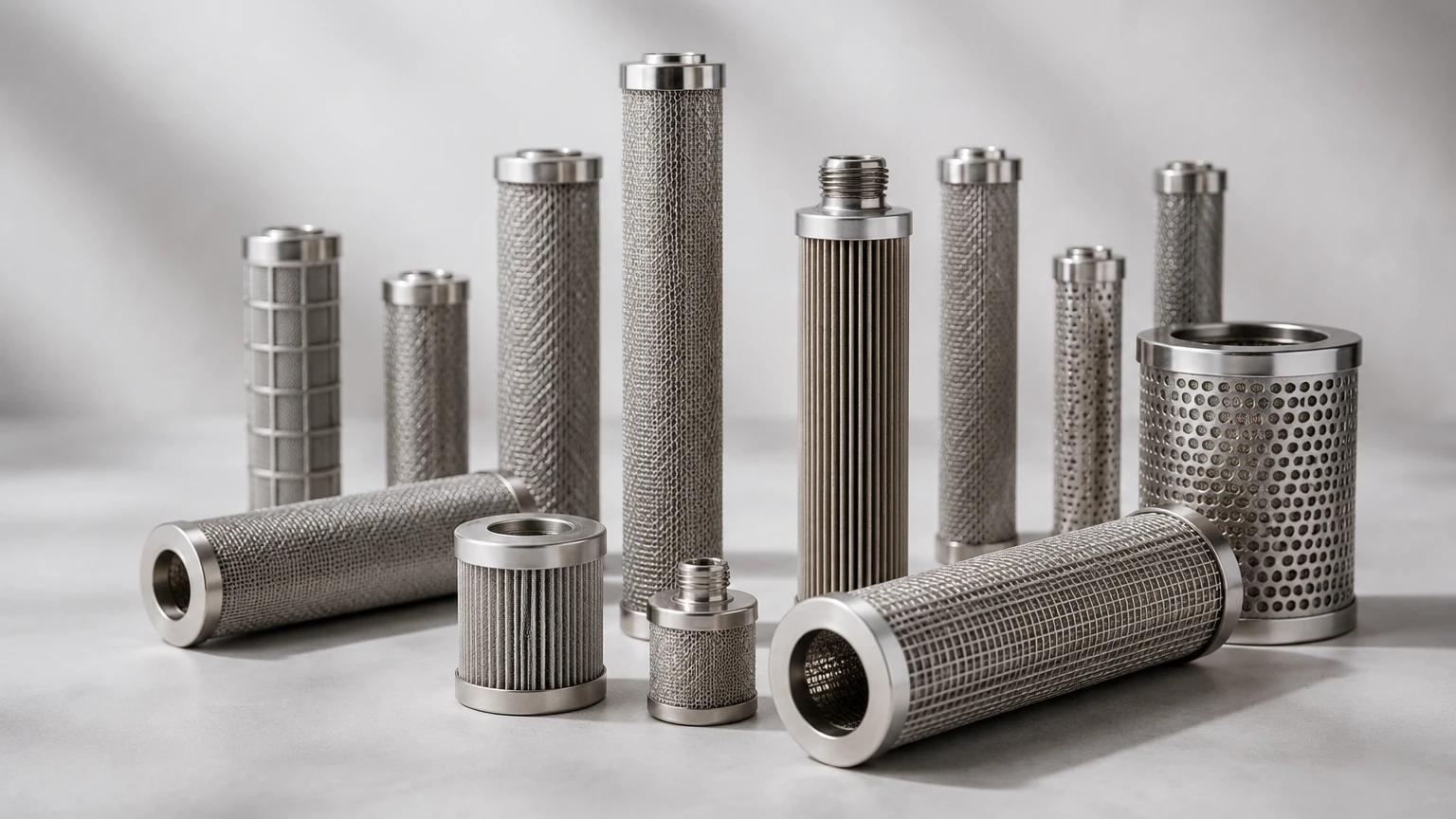
Customization and OEM Integration for Semiconductor Gas Systems
No two semiconductor fabrication plants (fabs) are identical, and the gas delivery requirements for an ALD (Atomic Layer Deposition) tool differ significantly from those of an ion implanter. Consequently, customization is a core requirement for gas purifiers in the semiconductor sector.
Tailored Housing Designs
OEMs often require purifiers to fit within specific footprints or to integrate directly into gas sticks or gas cabinets. Custom stainless steel housings can be engineered with specific inlet/outlet configurations, such as VCR® (Vacuum Coupling Radius) fittings, which are the industry standard for leak-tight, high-purity connections.
Application-Specific Media
The choice of filtration media must be compatible with the specific gas chemistry. For example, while 316L is suitable for most applications, certain highly corrosive halide gases may require nickel-based alloys or specialized surface coatings to prevent halogen-induced stress corrosion cracking. Engineering a custom solution involves analyzing the gas composition, flow dynamics, and expected temperature fluctuations to ensure the filter component does not become a point of failure.
Maintenance, Lifespan, and Total Cost of Ownership (TCO)
While gas purifiers for semiconductor applications are designed for longevity, they are ultimately consumable components. The lifespan of a purifier is determined by the capacity of its chemical media and the particulate loading of its filter element.
Replacement Indicators
In a B2B industrial setting, waiting for a process failure is not an option. Engineers typically monitor the lifespan of a gas purifier through:
- Pressure Drop Monitoring: An increase in ΔP across the purifier indicates particulate buildup in the final filter stage.
- Downstream Analytical Monitoring: Continuous or periodic sampling of the gas stream for moisture or oxygen breakthrough.
- Calculated Capacity: Based on the known contaminant levels in the source gas and the total volume of gas processed.
Total Cost Considerations
The TCO of a gas purifier includes the initial purchase price, the cost of installation (including helium leak testing), and the cost of downtime during replacement. High-quality stainless steel filters and purifiers may have a higher upfront cost, but their ability to withstand aggressive purge cycles and maintain low outgassing rates significantly reduces the risk of expensive wafer scraps, which can cost hundreds of thousands of dollars per batch.
Common Risks and Quality Assurance in Purification
The most significant risk in semiconductor gas purification is "bypass leakage." If the internal filter element is not perfectly sealed within the housing, contaminated gas can bypass the purification media and the filter, entering the process tool directly.
Leak Integrity
Every UHP gas purifier must undergo rigorous helium leak testing. A typical specification is a leak rate of less than 1 x 10^-9 atm-cc/sec. This ensures that no atmospheric oxygen or moisture can diffuse into the purifier and that no toxic process gases can escape into the fab environment.
Cleanroom Manufacturing
To meet the standards for "gas purifiers semiconductor" applications, the assembly of the filtration components must take place in a controlled environment, typically a Class 100 (ISO 5) or Class 10 (ISO 4) cleanroom. This prevents the introduction of environmental particulates during the manufacturing process itself. After assembly, the components are often vacuum-baked to remove residual moisture and then double-bagged in high-purity packaging.
Conclusion: Selecting a Partner for Semiconductor Filtration
Gas purification is a fundamental pillar of semiconductor manufacturing. The transition to smaller nodes and new materials (like High-k dielectrics) only increases the demand for ultra-pure gas delivery. For engineers and procurement teams, the focus must remain on the technical integrity of the filtration components—prioritizing material purity, surface finish, and proven filtration efficiency.
By understanding the engineering nuances of sintered metals and the stringent requirements of UHP environments, manufacturers can provide the reliable, high-performance solutions needed to keep the semiconductor industry moving forward. Whether you are designing a new gas cabinet or optimizing an existing process, the quality of your gas purifier is a direct determinant of your process success. For more information on custom filtration solutions and engineering support, visit our Main Page to explore how precision manufacturing supports the most demanding industrial applications.
